

New Delhi : In a major push toward self-reliance in semiconductors, the Government of India has enabled nationwide access to advanced chip-design technologies for academic and research institutions — a scale that officials say has not been seen anywhere else in the world.
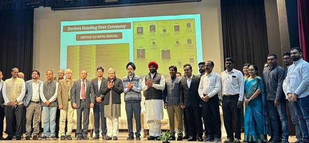
Union Minister for Electronics & Information Technology, Shri Ashwini Vaishnaw, on Friday handed over 28 fabricated chips (including 600 bare dies and 600 packaged chips) to students from 17 academic institutions during a ceremony at the Semiconductor Laboratory (SCL), Mohali, under the Chips to Start-up (C2S) Programme. The Minister also reviewed ongoing modernization activities at SCL.
Speaking at the event, Vaishnaw said India is rapidly emerging as a distinctive leader in the global semiconductor ecosystem.
“Institutions across the country today have access to some of the world’s most advanced semiconductor design technologies. This kind of large-scale semiconductor development ecosystem is unique to India,” he noted.
Record Design Participation Across India
According to the Ministry of Electronics & Information Technology (MeitY), the government has democratized chip design by equipping universities with industry-grade Electronic Design Automation (EDA) tools and Multi-Project Wafer (MPW) fabrication services.
Over the past one year:
- 5 MPW shuttles were completed at SCL Mohali
- 122 chip designs (tapeouts) were submitted
- 46 institutions across India participated
Of these, 56 student-designed chips have already been fabricated and delivered to respective institutions. MPW Shuttle Date Designs Institutions I 06 Dec 2024 20 17 II 28 Feb 2025 14 12 III 31 May 2025 22 15 IV 31 Aug 2025 38 20 V 30 Nov 2025 28 24 Total — 12246
ChipIN Centre Becomes One of the World’s Largest Centralized Chip-Design Facilities
A key component of this national semiconductor initiative is the ChipIN Centre, one of the largest design support hubs in the world, located at C-DAC Bangalore.
In the last year:
- Over 380+ organizations used the facility
- EDA usage surpassed 175 lakh hours
- 125 lakh hours — academic institutions (1 lakh+ students)
- 50 lakh hours — 90+ startups
The centre provides:
- Full chip-design toolchain
- Compute and hardware infrastructure
- IP cores
- Design mentorship
- Comprehensive fab support and packaging access at SCL
ChipIN ensures fab compliance and design review before sending student chips to fabrication, grouping multiple designs into a single MPW reticle, significantly lowering cost and time.
A Roadmap to Semiconductor Self-Reliance
Highlighting the vision of Prime Minister Narendra Modi, the Minister said India aims to build semiconductor capabilities of global scale and strategic independence.
“We must ensure that India does not depend on anyone else for its strategic needs. Our goal is to design and use indigenous chips, and SCL will play a crucial role in achieving this,” Vaishnaw emphasized.
As ChipIN Centre evolves into a value chain aggregator for advanced nodes, the government expects the C2S Programme to fuel innovation, support R&D, boost semiconductor startups and strengthen India’s journey toward becoming a major global semiconductor power.